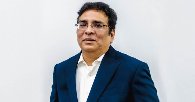
No room for dumb connected devices anymore: Balajee Sowrirajan


Samsung Semiconductor India Research (SSIR), a subsidiary of Samsung Electronics, has more than 4,000 employees. SSIR has contributed to many of Samsung’s global innovations including the Exynos chip, the world's first 108 megapixel camera and some phone sensors. In an interview, Balajee Sowrirajan, corporate vice-president and managing director of SSIR, talks about the company's progress, innovations, and trends shaping the industry. Edited excerpts:
How is SSIR contributing to the overall innovation at Samsung Electronics?
Globally, Samsung Semiconductor comprises three major business units -- Memory, Foundry, and System LSI (designing core semiconductors). Volatile memory (like static random access memory or SRAM and dynamic random access memory or DRAM) requires power to maintain data, while non-volatile memory (solid-state drive or SSD) does not need power to retain information stored in the chip. We have been building DRAMs for more than 30 years. But we work more on the non-volatile memory storage solution space such as SSD drives.

Please provide some examples.
Many of Samsung’s innovations were born at SSIR. One of Samsung’s flagship products, for which the end-to-end ownership and development is driven out of SSIR, is our Exynos system-on-a-chip (integrated circuit, or IC, design that combines elements of an electronic device onto a single chip) that is equipped with a 5G modem and neural network processing unit (for artificial intelligence or AI applications) and powers mobile devices and cars too. Our ISOCELL image sensors, too, use advanced pixel technology to power the cameras in your phones and cars.
At SSIR, we tune and qualify sensors, memory and storage devices to ensure that they function well under all conditions (like severe heat, biting cold, rough weather, etc). Further, sensors in many of the commercially-available phones globally have been designed at SSIR.
Moreover, the world’s first 108MP (megapixel) camera was planned and created by the engineers at SSIR--from designing the specification, hardware design and final software development. SSIR is also among the first to adopt a more advanced transistor architecture, as we (at Samsung Foundry) continue to establish our leadership with the production of the 3nm (nanometre) process node applying Gate-All-Around (to improve performance, reduce power consumption, and increase transistor density).

Have you filed any patents for the same?
SSIR has filed more than 1000 patents worldwide and more than 450 have been granted so far.
Are you able to source enough quality engineering talent from India?

We have well-trained talent in our campuses. When we recruit, we gauge their understanding of semiconductor device physics, digital design, basics of software, etc., along with their problem solving and analytical abilities. We spend close to six months to one year right on training them when they come from campuses. But our employees have to continuously improve themselves while we too have to upskill our people, especially given the rise of the use of AI and ML in our industries.
In this context, how is SSIR leveraging AI and ML?
Among other things, we use AI-ML for our design activity -- for example, how soon can I debug a problem? We can speed up the learning process with AI-ML techniques instead of doing things manually. Second, most of our applications have neural processing units that help algorithms to run very fast.

SSIR is partnering with the Indian Institute of Science (IISc) to promote R&D in the field of on-chip Electrostatic Discharge (ESD) Protection. What does it entail?
Collaborating with some academic institutions is very important for us to push our innovation research to the next level. Practically every electronic system comprises Integrated Circuits (ICs) and SOCs but they are very sensitive to ESD failures (release of stored static electricity can damage these sensitive equipment). IISc is one of the few institutes in the world leading ESD device research. The collaboration is aimed at helping us jointly develop highly-reliable interfaces and SoCs that operate at low power and high speed. This is a multi-year project, and hopefully it will open more opportunities for research with them.
Can you elaborate on the IoT opportunity for semiconductor companies with the insistence on smart cities, smart homes, and smart factories?

I'm no longer talking about just the Internet of Things (IoT) but also the Intelligence of Things. This is because AGI (artificial general intelligence) is becoming a very important aspect, which leaves no room for dumb connected devices. You now want a lot of decisions to be made on the edge (closer to the devices rather than on a distant server) — say on your phones or your automobiles.
But this also implies that you will need lower latency for mission critical applications like cars, medical equipment, etc.
We have a lot of innovations on that front, specifically on the modem side. These are modems not only for phones — your refrigerators would have a modem in the future, and every device will have a modem and some kind of a neural processing unit or an AI-ML (machine learning) processing unit, which will also make power management a very important requirement. Further, sensors might not just be for photographs but will also be used in many areas like light and smell sensors which may play a very big role in the future.

What more should India do to become a global innovation hub and encourage more 'Make AI in India make AI work from India'?
India already has a big local (semiconductor) design ecosystem. As for AI, I think there has to be a lot of design models or design use cases. It's not just about chip design but more on the product design. We have to start from the top of the value chain and introduce products systematically for India.
